Integrated subsystem optimized for customer applications including chiplets
Cadence (Nasdaq: CDNS) today announced the tapeout of the industry’s first LPDDR6/5X memory IP system solution optimized to operate at 14.4Gbps, up to 50% faster than the previous generation of LPDDR DRAM. The new Cadence® LPDDR6/5X memory IP system solution is a key enabler for scaling up the AI infrastructure to accommodate the memory bandwidth and capacity demands of next-generation AI LLMs, agentic AI and other compute-heavy workloads for various verticals. Multiple engagements are currently underway with leading AI, high-performance computing (HPC) and data center customers.
This press release features multimedia. View the full release here: https://www.businesswire.com/news/home/20250709175651/en/
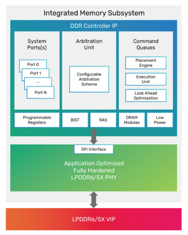
Cadence LPDDR6/5X system solution example
The Cadence IP for the JEDEC LPDDR6/5X standard consists of an advanced PHY architecture and a high-performance controller designed to maximize power, performance and area (PPA) while supporting both LPDDR6 and LPDDR5X DRAM protocols for optimal flexibility. The solution supports native integration into traditional monolithic SoCs as well as multi-die system architectures by leveraging the Cadence chiplet framework, enabling heterogeneous chiplet integration. The chiplet framework, including the previous LPDDR generation, was successfully taped out in 2024.
“The evolution of data centers from HPC compute virtualization to AI training and inference at scale has driven a massive buildout of AI infrastructure, and designing for efficient data movement via memory interfaces has never been more crucial. LPDDR6 has emerged as a key enabler of accelerated compute, providing the speed, bandwidth, power profile and capacity needed to efficiently perform AI inference,” said Boyd Phelps, senior vice president and general manager of the Silicon Solutions Group at Cadence. “With this tapeout, Cadence is continuing our track record of memory IP leadership by offering an industry-first LPDDR6 implementation delivered as an integrated subsystem optimized for customer applications.”
The complete PHY and controller memory system boasts a new high-performance, scalable and adaptable architecture based on Cadence’s proven and highly successful DDR5 12.8Gbps, LPDDR5X 10.7Gbps and GDDR7-36G product lines. This first offering in Cadence’s new LPDDR6 IP product line supports the LPDDR6 and LPDDR5X standards, including LPDDR5X CAMM2.
Suitable for the AI, mobile, consumer, enterprise HPC and cloud data center markets, the advanced LPDDR6/5X memory IP system solution allows maximum flexibility for end products with a range of performance, capacity and cost targets—ensuring long production runs. The LPDDR6/5X PHY is customizable for different package and system topologies and available as a drop-in hardened macro. This ensures fast and reliable integration, translating into rapid time to market.
The Cadence LPDDR6/5X controller includes a full set of industry-standard and advanced features for memory interfaces, such as support for the Arm® AMBA® AXI bus. The memory controller is provided as a soft RTL macro for maximum flexibility in features, power, area and performance.
The Cadence LPDDR6 solution includes the LPDDR6 Memory Model, which enables engineers to perform comprehensive verification and ensure that system-on-chip (SoC) designs are compatible with the latest JEDEC interface standard, accelerating their adoption of this new technology with confidence. The LPDDR6 Memory Model includes a complete set of protocol checks, functional coverage and a verification plan.
Available now for customer engagements, the new LPDDR6/5X IP is the latest addition to Cadence’s comprehensive family of memory IP system solutions, which also includes DDR, GDDR and HBM. Cadence Memory IP is designed with the company’s industry-leading analog/mixed-signal design tools. When combined with Cadence’s UCIe™-based chiplet framework, the new LPDDR6/5X IP and Cadence’s other leading memory and interface IP deliver an optimized solution that enables rapid chiplet realization. For more information on the new LPDDR6/5X IP, please visit the LPDDR landing page on cadence.com.
About Cadence
Cadence is a market leader in AI and digital twins, pioneering the application of computational software to accelerate innovation in the engineering design of silicon to systems. Our design solutions, based on Cadence’s Intelligent System Design™ strategy, are essential for the world’s leading semiconductor and systems companies to build their next-generation products from chips to full electromechanical systems that serve a wide range of markets, including hyperscale computing, mobile communications, automotive, aerospace, industrial, life sciences and robotics. In 2024, Cadence was recognized by the Wall Street Journal as one of the world’s top 100 best-managed companies. Cadence solutions offer limitless opportunities—learn more at www.cadence.com.
© 2025 Cadence Design Systems, Inc. All rights reserved worldwide. Cadence, the Cadence logo and the other Cadence marks found at www.cadence.com/go/trademarks are trademarks or registered trademarks of Cadence Design Systems, Inc. Arm and AMBA are registered trademarks of Arm Limited (or its subsidiaries) in the US and/or elsewhere. UCIe is a trademark of UCIe Consortium. All other trademarks are the property of their respective owners.
Category: Featured
View source version on businesswire.com: https://www.businesswire.com/news/home/20250709175651/en/
The evolution of data centers from HPC compute virtualization to AI training and inference at scale has driven a massive buildout of AI infrastructure, and designing for efficient data movement via memory interfaces has never been more crucial.
Contacts
For more information, please contact:
Cadence Newsroom
408-944-7039
newsroom@cadence.com